Optimal SMA Launch Layout
Introduction
We’ve recently been working on several compact, robust, and cost effective time domain reflectometers (TDR) devices for integration into larger systems. Our most recent one, the TDR01, has 60ps sampled edges with a unit cost under $15 which we were pretty happy with. This version is a bit more fully featured then our single diode sampler. Phil has a post up on EOI’s page about the project here. We’re working on releasing those as a headless USB controlled model later this year, get in touch if you’re interested in evaluating those.
Since we’re targeting OEM use and test equipment we wanted to see how good we could get with less expensive connectors. Sure you can get arbitrarily nice SMAs but there are some downsides including limiting sourcing options and form factors not to mention BOM cost.
So lets see how good we can get with a standard edge mount SMA like this Samtec SMA-J-P-H-ST-EM1.
Resources
If you find this article interesting checkout Ted Yapo’s Hackaday which is wonderful and I wish I’d found it earlier! His testing is extremely through and well documented.
There’s a good paper on the same topic as this post here.
When writing this I came across Hans Rosenberg’s Video Series on RF PCB design which is worth a watch. He uses the nanoVNA to make some related measurements which is a great device especially for a few hundred bucks.
This guide from Cinch gives through assembly instructions for edge mount SMAs. There’s assembly considerations that you won’t be prepared for if you’re working on your first RF board.
The Problem

Recommend footprint of Samtec SMA-J-P-X-ST-EM1.

Recommend footprint of Samtec SMA-J-P-X-ST-EM1.
Lets use the Oshpark stackup as an example. For a dielectric of 3.61 and prepreg height of 7.87 mil our 50 \( \Omega \) trace should be 15 mil (microstrip). Digikey’s solver is a useful tool and the IPC 2141 spec is a good read explaining the calculations.
The Samtec pad width suggestion is 50 mil (>3x our 50 \( \Omega \) trace width!). Combined with the pin width and the proximity to the ground pins and pads this will give a low impedance section and will cause reflections in our TDR.
There’s a decent overview of this problem from TI here. It doesn’t go into the depth that you really want but it sets up the problem with some included measurements.
On a suggestion from Highland Technology’s ever capable John Larkin we tried out the ATLC2: Arbitrary Transmission Line Calculator to simulate the impedance.
This is a bit faster than setting up an Finite Difference Time Domain (FDTD) simulation by a country mile but still give the introduction a read. I did the layout in Inkscape all in pixel units with a spreadsheet for the unit translation.
First Demo
As a starting point I threw together a simple version using the default materials map.

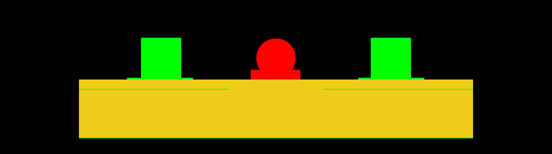
Small demo version of a microstrip line with soldermask.
Small demo version of a microstrip line with soldermask.
Comparing to the IPC 2141 estimation of 53.6 \(\Omega\) we get an acceptable discrepancy of 0.15 \( \Omega \).
This instills a certain confidence in the method!
Modeling the SMA
To model this in ATLC2 (and other meshed methods like FDTD) we need to define our box size and then our objects in units of those boxes.
| Measurement | Pixels | Target (mm) | Actual (mm) |
|---|---|---|---|
| Trace height | 2 | 0.035 | 0.035 |
| Trace width | 20 | 0.35 | 0.35 |
| Mask height | 6 | 0.1 | 0.105 |
| Dielectric height | 12 | 0.2104 | 0.21 |
| Separation | 11 | 0.192 | 0.1925 |
| Core height | 61 | 1.065 | 1.0675 |
| L2 height | 1 | 0.0175 | 0.0175 |
| SMA ground lead width | 63 | 1.1 | 1.1025 |
| SMA ground trace width | 86 | 1.5 | 1.505 |
| SMA ground lead sep. | 240 | 4.2 | 4.2 |
| SMA conductor diameter | 51 | 0.9 | 0.8925 |
| Ground relief | 100 | 1.75 | 1.75 |
| SMA ground pad sep. | 206 | 3.6 | 3.605 |
These values give us a bitmap that looks like this which we use directly as the input to the simulator.
Input file to ATLC2. The material type is encoded in the colour and the simulation boxes are pixels. The center conductor thickness is an approximation of the solder fillet.
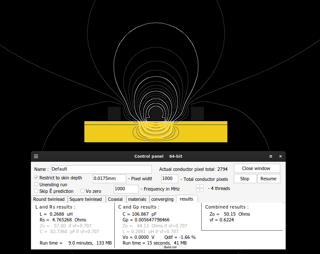
Adding a layer two ground plane relief under the center conductor reduces capacitance and adds some inductance giving us a much closer impedance.
Running a simulation for the default case with no relief in the ground plane gives us a huge impedance mismatch.
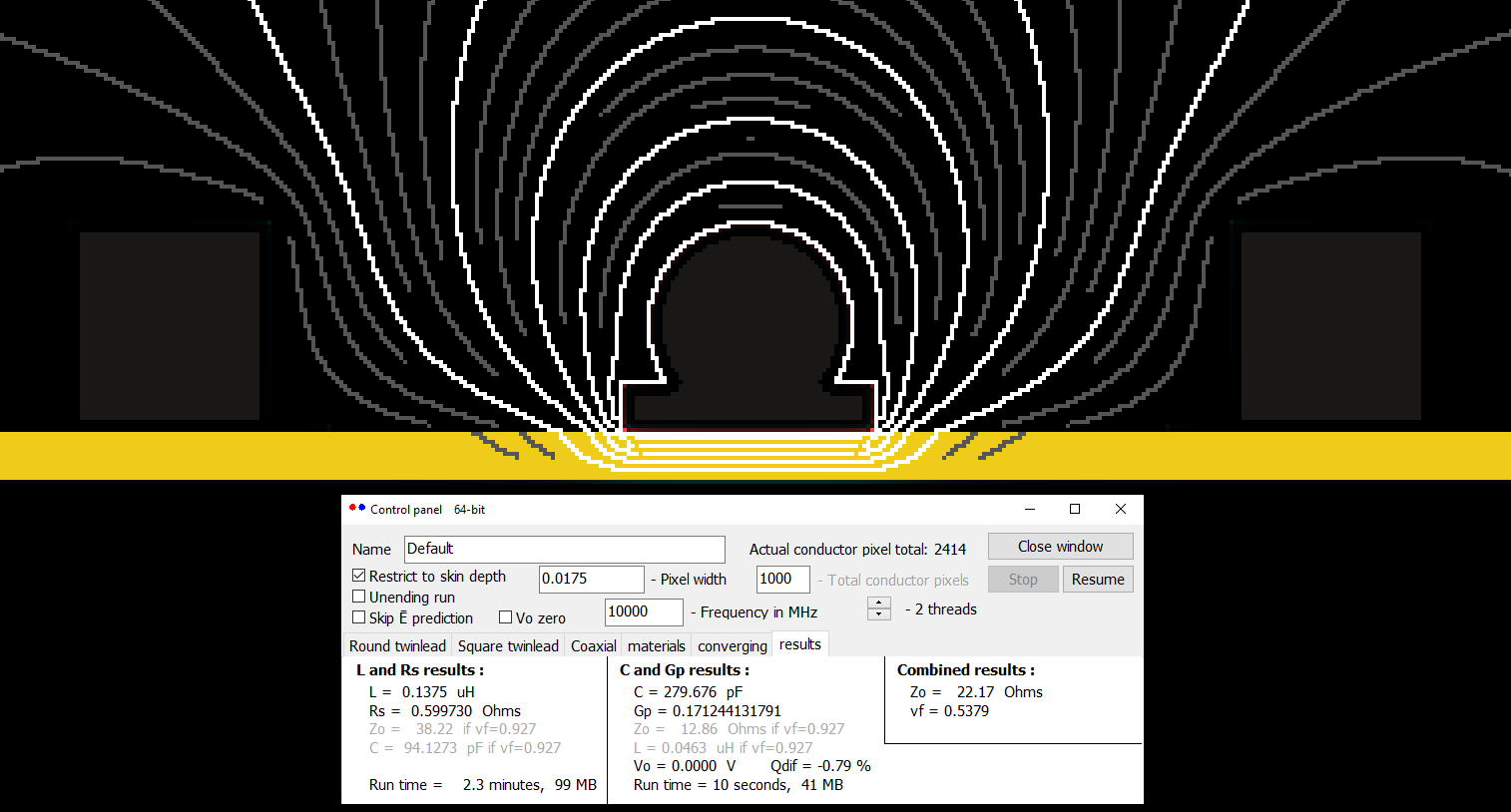
Without the relief our capacitance is a bit high giving a impedance of just 22 Ohms.
| Configuration | Z (Ω) |
|---|---|
| No ground relief (simulated) | 22 |
| With ground relief (simulated) | 50.15 |
| Measured | 49 |
Conclusion
You can seriously decrease the impedance discontinuity at your connector by adding some ground plane relief. Unfortunately I don’t have any plots I can share but we measured 49 ohms and drastically decreased reflections at the connector.
Plans are to add a head to head with the different edge mount SMA types with a focus on the time domain performance. Making the standard connectors perform better will lower costs, offer more sourcing options, and git us more form factors so it’s worth a bit more investigation!