Pin 1 Markings and PCB Assembly
Categories:
Most pick and place files are programmed by hand. Remember this and repeat it to yourself whenever you’re checking your files for PCBA manufacturing.
Chris Denny’s KiCON 2019 talk is essential viewing on this topic—he breaks down the manual process behind pick-and-place programming and how subtle mistakes can creep in.
Assembly layers are a great utility to supplement the silkscreen and help the person programming the pick-and-place machine. We want to make their lives as easy as possible to reduce surprises on the production line.
For reference designators, KiCad’s default—placing the reference designator on the assembly layer directly under the part—is a huge help.
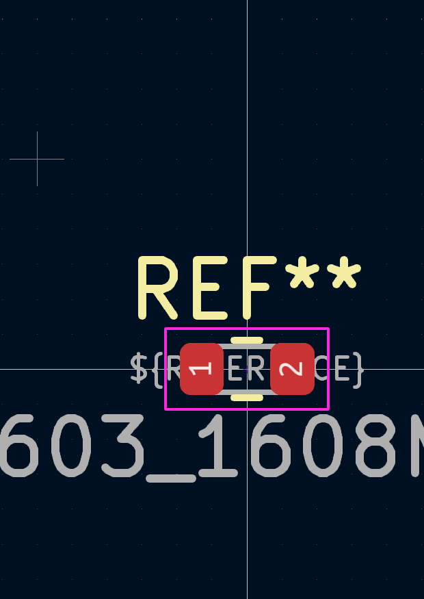
0603 Library Footprint
Silkscreen gets tricky on tightly packed boards. You often need to move parts, and end up relocating designators away from the actual components.
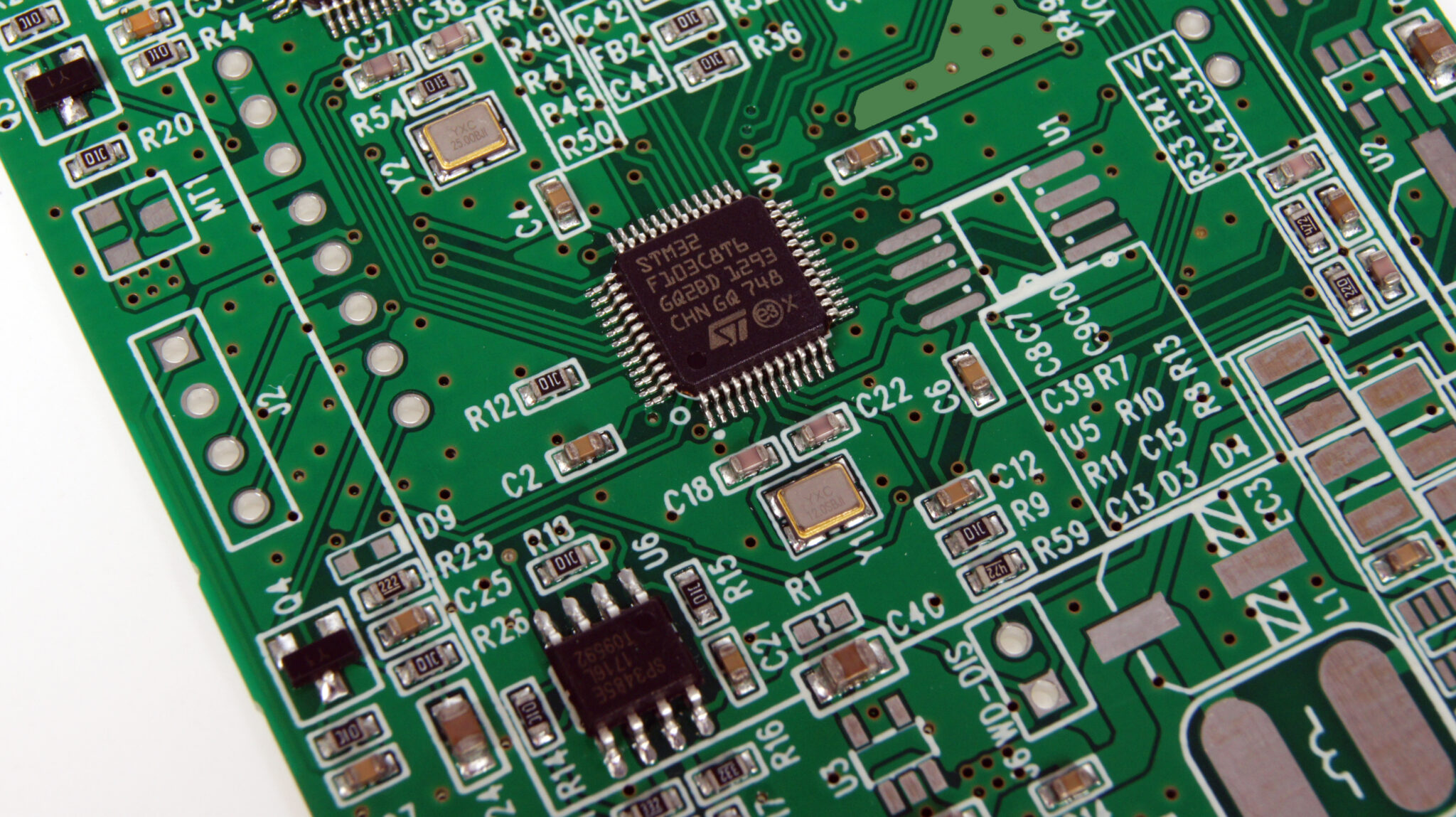
Silkscreen for tightly placed parts
This can be ambiguous. It’s easy to get misled—especially when you’re inspecting or debugging a board. Leaving the reference on the assembly layer, directly under the part, avoids this entirely when looking at the gerbers.
Years ago, I was using DipTrace—which doesn’t make using the assembly layer easy. The silkscreen was misleading, and I ended up with several hundred boards with two passives swapped even though they were correct on the centroid.
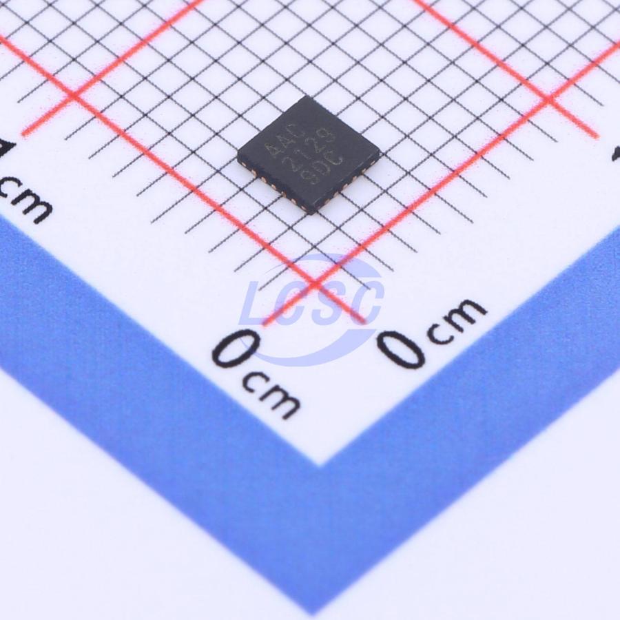
Today, I Have a Far Worse Issue: Rotated QFNs
QFNs are commonly rotationally symmetrical so there are four ways to place the component, three of them are wrong. I was using a footprint from KiCad’s QFN library and I’ll just say it: This is not a good Pin 1 marking on the silkscreen.
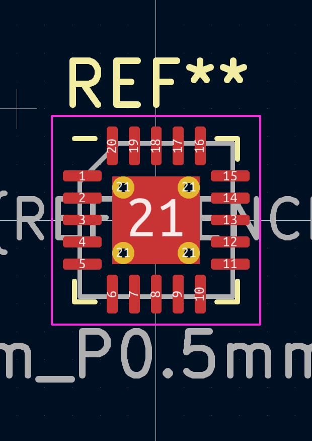
KiCad QFN from library
Some CAD programs don’t make use of the assembly layer at all—so silkscreen becomes the first and last line of defense.
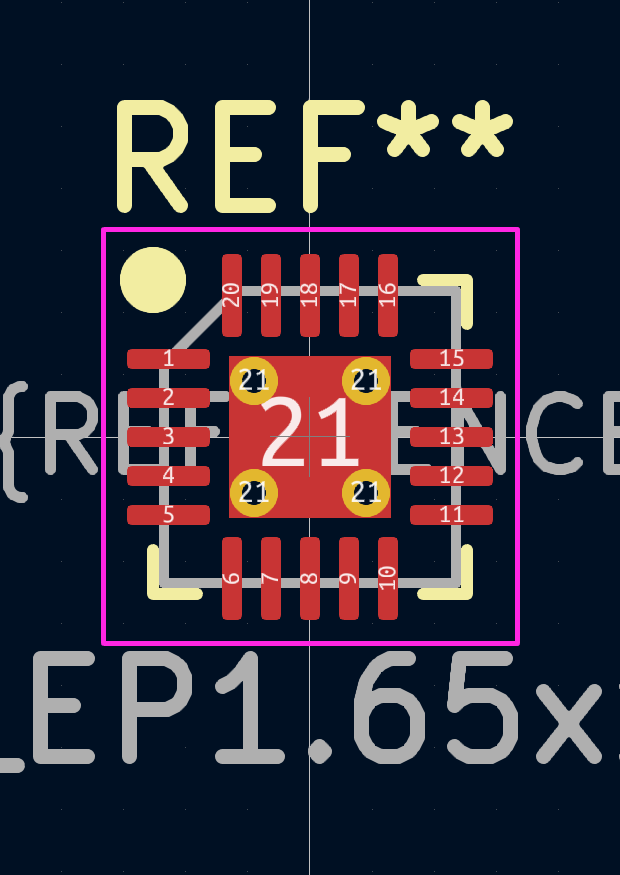
Improved QFN pin one marking
Here’s the improved footprint. You can’t miss that pin one marking, any mistakes are enemy action. Guess which version my design was using?
Yep—the original, barely-there silkscreen mark. The assembly layer wasn’t used by the assembler. The centroid file was correct. The alignment step was correct. The assembled boards are wrong.
I will be making my markings as obvious on the silkscreen as possible from here on out. Now I’ve got to sort out a few hundred QFNs with the wrong orientation.
Update
It happened again with the updated silkscreen on the same board.
Microchip MCP3564T
Everything in the design files was correct—but the part was still loaded incorrectly. The package itself is symmetrical and lacks a clear physical Pin 1 indicator. This time, I’m blaming Microchip.